Custom Semiconductor Parts CNC Machining – Ultra-Precision Components for High-Tech Applications
Introduction: The Demand for Precision in the Semiconductor Industry
The semiconductor industry is one of the most precision-driven sectors in modern manufacturing. From wafer processing to chip packaging and photolithography, every component in a semiconductor tool must meet ultra-tight tolerances, exhibit chemical and thermal stability, and maintain dimensional accuracy under extreme operating conditions.
As a trusted partner in custom semiconductor parts CNC machining, we specialize in producing high-precision, cleanroom-compatible components based on customer-provided drawings. Our capabilities support both prototyping and volume production for semiconductor equipment OEMs, system integrators, and cleanroom tool manufacturers.
Machining Challenges and Our Solutions
Manufacturing components for semiconductor equipment involves a unique set of challenges:
- Extreme Tolerance Requirements: Precision of ±0.001mm or better is often mandatory, especially for wafer-handling arms, optical housings, and positioning systems.
- Cleanroom Compatibility: Parts must be free from contaminants and particulates, with strict adherence to surface finish and material purity standards.
- Complex Geometry and Thin-Wall Designs: Many parts, such as gas manifolds and vacuum chambers, involve intricate cavities, ports, and internal channels requiring multi-axis machining.
- Material Sensitivity: Materials used in semiconductor processing (e.g., ceramics, aluminum alloys, and engineering plastics) require tailored tooling, coolant strategies, and contamination control.
Our Solution:
We deploy a comprehensive precision machining process with state-of-the-art 5-axis CNC machines, high-purity material handling, and cleanroom-safe finishing techniques. Our engineers collaborate with clients from the design stage to optimize manufacturability and surface specifications, ensuring compliance with semiconductor-grade standards.
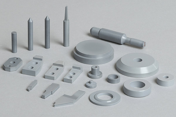
Commonly Used Materials and Their Characteristics
Due to the sensitive nature of semiconductor manufacturing environments, material selection is critical. We routinely machine the following materials:
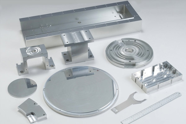
- Aluminum Alloys (6061-T6, 5052, 7075): Lightweight, corrosion-resistant, and suitable for vacuum chambers, frames, and gas panels.
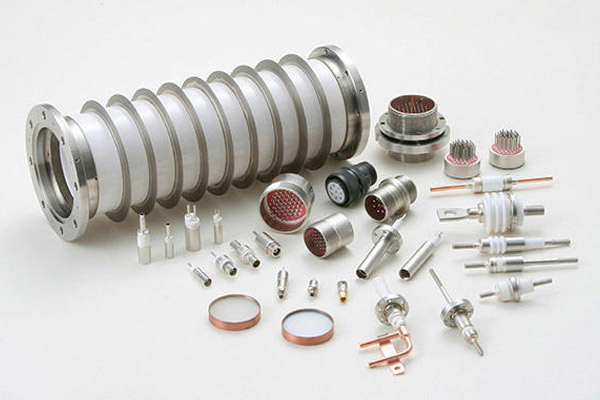
- Stainless Steel (316L, 304, 303): High corrosion resistance and low outgassing, ideal for wet benches and high-purity fluid systems.
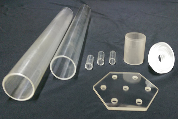
- Engineering Plastics (PEEK, PTFE, PPS, POM): Chemically resistant and thermally stable, used for insulators, fluid connectors, and non-metallic bearings.
- Ceramics (Alumina, Zirconia): Extremely hard and thermally stable, suitable for plasma chambers, etching components, and wear-resistant fixtures.
- Titanium (Grade 2, Grade 5): Excellent strength-to-weight ratio and corrosion resistance, used in precision structural parts for vacuum environments.
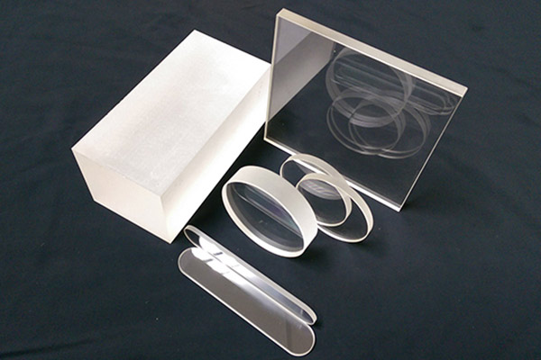
- Quartz and Glass Components (by partner fabrication): For optical modules and photolithography applications.
Each material is handled in accordance with semiconductor manufacturing standards to minimize contamination, ensure uniformity, and maintain batch-to-batch consistency.
CNC Machining Capabilities
As a provider of custom semiconductor parts CNC machining, our workshop is fully equipped to meet the industry’s stringent requirements:
- Precision and Tolerances:
- Dimensional control: ±0.001mm
- Surface finishes: Ra 0.2μm to Ra 0.05μm for sealing and bonding surfaces
- Flatness and roundness: ≤0.002mm, verified by optical and contact methods
- Machinery and Inspection:
- Mikron 5-axis CNC Machining Centers: Ideal for complex components and fine-featured parts
- Mazak CNC Lathes: For high-precision turning of bushings, flanges, and ring-type components
- Studer CNC Grinders: For ultra-fine finishing of wear-critical surfaces
- Zeiss CMM & Tokyo Seimitsu Roundness Testers: Comprehensive quality control of geometry and surface quality
- Clean inspection area and contamination-free packaging line
- Support Services:
- Anodizing, electropolishing, and passivation for aluminum and stainless steel
- Ultrasonic cleaning and vacuum sealing for cleanroom delivery
- First Article Inspection (FAI), PPAP, and material certification (ROHS, REACH)
All parts are machined to exact customer specifications and delivered in clean, traceable packaging suitable for Class 100–1000 environments.
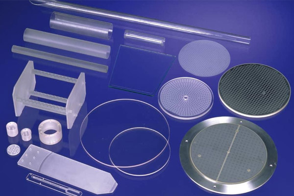
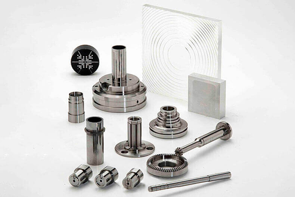
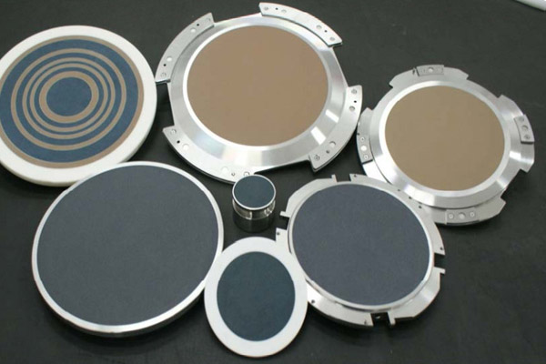
Typical CNC Machined Parts and Applications
We manufacture a wide range of custom CNC machined parts for the semiconductor industry, used in equipment such as wafer handlers, deposition systems, photolithography tools, and metrology instruments:
- Wafer Transfer Arms and Holders: Ultra-flat and chemically inert parts for wafer manipulation
- Vacuum Chamber Flanges and Rings: High-precision components for vacuum integrity
- Gas Manifolds and Flow Channels: For process gas distribution in CVD, ALD, and etching equipment
- Sensor Housings and Mounts: For alignment and detection systems in lithography and inspection tools
- Tool Frames and Chassis Components: Lightweight and stable structures for semiconductor assembly platforms
- Nozzles, Fixtures, and Plates: Custom machined for wafer cleaning, spin-coating, or plasma exposure systems
Each part is produced according to customer CAD drawings or 2D technical specifications, with full dimensional and surface inspection before shipment.
Project Highlight
In a recent collaboration with a global semiconductor OEM, we manufactured a batch of PEEK wafer retainers with a ±0.002mm tolerance and Ra 0.1μm surface finish on contact surfaces. These components were laser-etched with part traceability codes and vacuum-packed in ISO-class cleanroom conditions, ensuring direct integration into the client’s Class 1000 production environment.
Your Trusted Partner for Semiconductor Precision Machining
The semiconductor industry demands nothing less than perfection—both in process and in product. Our custom semiconductor parts CNC machining services are designed to support your cleanroom-critical, high-spec projects with unmatched accuracy and quality assurance.
Reach out to us today with your drawings or specifications. Whether you’re developing a new wafer tool or scaling up high-purity component production, we’re here to deliver precision components that meet your timeline, quality, and innovation goals.