
Precision Machining & Ceramic Component Solutions for Semiconductor Manufacturing
Semiconductor fabrication demands ultra-high precision, exceptional material purity, and tooling that withstands extreme heat, pressure, and chemical exposure. Our specialist machining services produce semiconductor-grade components—from ceramic wafer chucks to metal seals and mold parts—designed to meet stringent cleanroom and electrical requirements.
Key Manufacturing Capabilities
Industrial Ceramic & Technical Material Machining
We machine advanced materials including alumina (≥ 99.7% purity), zirconia, silicon carbide, silicon nitride, boron nitride, Y₂O₃ ceramics, sapphire, and quartz glass. Our process ensures structural strength, high temperature resistance, chemical stability, and minimal contamination.
Tungsten Carbide & Hard Material Components
Expertise in fabrication of non-magnetic, conductive carbide parts and high-strength alloy components used in packaging fixtures, alignment tools, and mold inserts—ensuring stability and performance in precision semiconductor equipment.
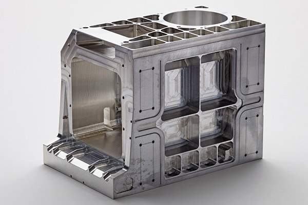
High‑Precision CNC Milling & Turning
Support for ultra-tight tolerance components machined via 3-, 4-, and 5-axis CNC, utilizing turning, milling, and large-format machining to produce critical parts like wafer suction pads, mold cavities, RF windows, lead frame dies, and structural mounts.
Micro‑Scale & Fine Feature Machining
Capability to machine microportions and fine holes—including micro-needles, capillaries, fine slots, and cavity profiles—required for wire-bond tools, capillary tubes, and die frames used in IC packaging.
EDM & Mirror Finish Wire-Cut Machining
Wire electrical discharge machining and spark EDM deliver high-precision cavities and mirror-surface finishes on dielectric ceramics and hard metals, ideal for molds, sealing faces, and ceramic RF windows.
3D Printing & Mold Prototyping
Rapid prototyping including polyurethane, metal, and ceramic 3D printing for mold components, such as lead frame fixtures, cavity blocks, molding inserts, and adaptive test fixtures.
Heat Treatment & Surface Finishing
Thermal Processing
Vacuum quenching, solution treatment, gas nitriding, tempering, aging, and stress relief applied to metallic tooling and mold components to ensure dimensional stability and wear resistance.
Surface Treatments
Advanced finishes including anodizing, chemical conversion coatings, passivation, electroless nickel plating, chrome plating, etching, dry-film lubrication, and painting—all engineered for contamination control and high-purity semiconductor environments.
Quality & Inspection Protocols
We adhere to materials and testing standards essential for semiconductor manufacturing:
- Material Traceability & High-Purity Standards for ceramics and metals
- Non-Destructive Testing (NDT) such as fluorescent penetrant inspection, X-ray, and magnetic particle testing for critical mold inserts and metal parts
- Surface Roughness Control to achieve low particle generation and optimal dielectric behavior
- Dimensional & Flatness Inspection for sealing surfaces, wafer carriers, and alignment fixtures within tight tolerances
Semiconductor Industry Applications
Our services support critical device manufacturing and packaging equipment:
- Wafer Handling and Vacuum Chucks: High-purity ceramic suction pads and fixtures
- Lead Frame and Mold Inserts: QFP, BGA, LQFP cavity blocks, terminals, cutting dies and mold cores
- RF & Thermal Components: Sapphire or quartz windows, ceramic insulating mounts, RF transmission plates
- Wire-Bond & Capillary Tools: Ceramic capillaries, micro-needles for ultrasonic bonding
- High-Performance Hardware: Ceramic pump seals, flow-control interfaces, non-magnetic alignment tools
SEO-Focused Keywords
Include these keywords across headers, metadata, alt tags, and body content to boost search engine ranking:
- Semiconductor ceramic machining
- High-purity alumina parts manufacturing
- Sapphire window machining for semiconductors
- Tungsten carbide mold inserts CNC machining
- Lead frame mold cavity machining
- Wire-bond capillary ceramic parts
- Precision quartz glass component machining
- Cleanroom grade ceramic tooling
- EDM mirror finish molds
- Semiconductor packaging mold machining
Why Choose Specialist Semiconductor Component Machining?
- Ultra‑High Purity & Contamination Control: All ceramic and metal parts are processed to semiconductor cleanroom standards
- Precision & Stability: Sub-micron flatness and parallelism for sensitive process equipment
- Multi‑Material Expertise: From sapphire and alumina to carbide and high-strength alloys
- End‑to‑End Production: From CNC machining and micro‑feature EDM to thermal treatment and polishing inspection
- Rapid Turnaround for Prototyping & Volume: Scalable to meet both R&D and production needs
Request a Tailored Quote
Have a design or need semiconductor-grade ceramic tooling, mold inserts, or alignment components? Submit your drawings and specifications to receive a tailored machining proposal—optimized for material properties, tolerance, surface finish, and environmental compatibility.