
Precision Machining for Semiconductor Packaging & Final Test Components
Enabling Reliable IC Testing and High-Yield Packaging with Sub-Micron CNC Expertise
At the final stage of semiconductor manufacturing, precision means everything. Whether it’s in probe cards testing 5nm chips, sockets exposing micro-pins to mechanical stress, or packages requiring perfect co-planarity — component integrity directly affects yield, signal integrity, and device lifetime.
With over two decades of CNC manufacturing experience, our China-based facility provides ultra-precise, cleanroom-ready components for leading packaging houses, test handlers, probe card manufacturers, and OSATs globally.
✔ Machining Difficulties in Packaging & Test Hardware
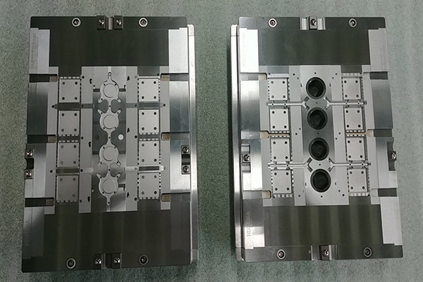
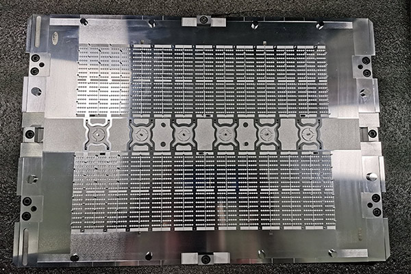
Packaging and test parts may look small — but their complexity and tolerance requirements are world-class:
- Micro-hole & micro-slot machining: Probe card plates often require holes <0.2mm with ±0.005mm positional accuracy.
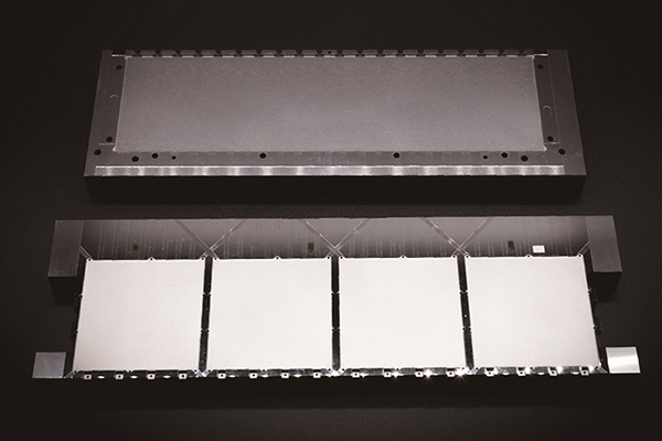
- Ultra-thin walls & micro features: High-density test sockets and stiffeners demand 0.2mm or thinner walls without deformation.
- High thermal & electrical performance: Materials must remain dimensionally stable under high temperature and cycling loads.
- Planarity & parallelism: Contact areas must maintain <0.01mm flatness across entire surfaces to ensure test signal reliability.
- Non-magnetic, ESD-safe, and low-particle surfaces: Especially critical in advanced node testing and Class 100 cleanrooms.
✔ Materials We Master for High-Precision Test & Packaging Parts
| Material | Common Use | Machining Focus |
|---|---|---|
| Ceramics (Alumina / Zirconia / Silicon Nitride) | Probe card stiffeners, contact blocks | Diamond tooling, non-chipping edge profiling |
| Super Engineering Plastics (PEEK, Torlon, Ultem) | Test sockets, inserts, isolation fixtures | Burr-free micro-drilling and ultra-clean chamfering |
| Tool Steel (SKD11, M2) | High-wear pins, jigs | Heat treated to HRC 60+, ground to <0.002mm tolerance |
| Beryllium Copper (BeCu) | Micro-spring holders, socket frames | Special alloy handling with surface passivation |
| Titanium Alloys | Probe card carriers | Ultra-lightweight and low thermal expansion |
| C1100 / OFHC Copper | Heat spreaders | CNC + polishing + Ni/Au plating for thermal/electrical performance |
All materials are traceable and RoHS/REACH compliant, with options for Ni plating, Au coating, black oxide, or PEEK overmolding.
✔ CNC & Finishing Capabilities Tailored for IC Test & Packaging
Our workshop integrates specialized processes to meet the micro-mechanical requirements of the test world:
- Micro-hole CNC Drilling (≤φ0.1mm) – With ±0.005mm positional tolerance
- EDM + Wire-Cut for Tool Steel & Titanium – For ultra-fine slots, edge profiling, sharp corners
- Mirror Surface CNC Milling & Lapping – Flatness < 0.005mm and Ra ≤ 0.1μm
- Diamond Grinding for Ceramics – Crack-free edge shaping and high-precision ID/OD grinding
- Assembly-Ready Finishing – Anodizing, electroless Ni/Au, and cleanroom packaging
Inspection Equipment Includes:
- Nikon Vision System for micro-feature inspection
- CMM + height gauge for planarity and parallelism
- X-ray coating thickness measurement (for plated layers)
- Surface profiler for burrs and Ra < 0.05μm
✔ Global Cases – We Build for the Final Step That Matters Most
- ✅ Precision ceramic probe card plates for a Japanese ATE system integrator
- ✅ PEEK ultra-thin IC socket frames for a U.S. OSAT company
- ✅ Beryllium copper contact modules for a Taiwan-based wafer-level test group
- ✅ Mirror-polished heat spreaders for advanced packaging in Singapore & Malaysia
We support rapid prototyping (under 7 days), small-volume pre-launch runs, and high-mix production for custom IC packages.
✔ Why Global Packaging & Test Leaders Work with Us
- 🏭 20+ Years of CNC experience with fine-feature, thin-wall, and hybrid material machining
- 📐 Micro-hole accuracy, ultra-flat surfaces, and full burr control
- 🧼 Cleanroom-ready finishing & packaging (Class 1000)
- 🔩 Support for assembled modules (e.g., ceramic + metal + polymer stacking)
- 🌍 Global delivery to fabs, OSATs, ATE and test socket manufacturers in 30+ countries
🧪 Let’s Make Your Final Stage Perfect — Contact-Ready, Burr-Free, Precision-Cut
Precision packaging and test components don’t just hold chips — they hold your yield rate, reliability, and reputation. Partner with us for CNC excellence you can measure in microns and trust in mass production.
📤 Upload your drawing today — receive a quote and DFM review within 24 hours.