Precision Machining for Wafer Fabrication Equipment Parts
Empowering Global Semiconductor Manufacturing with 20+ Years of CNC Expertise from China
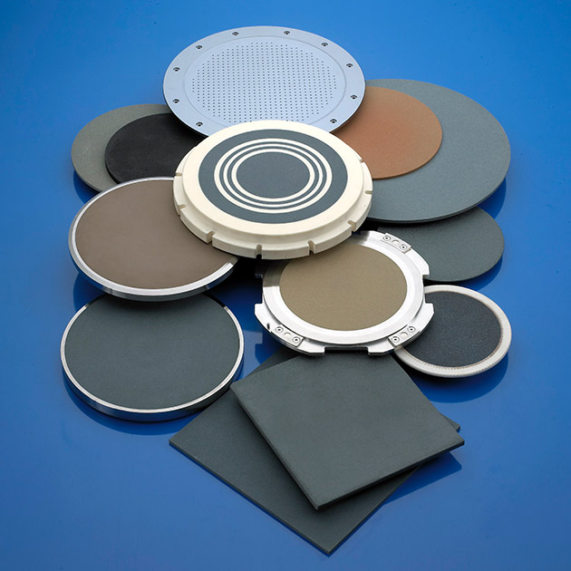
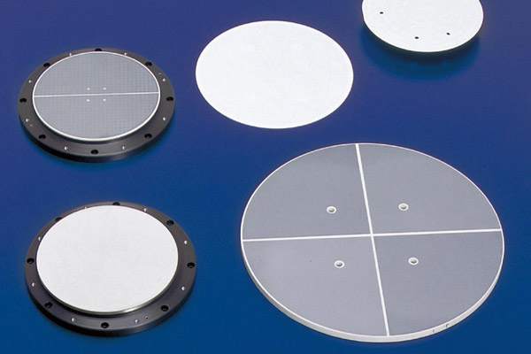
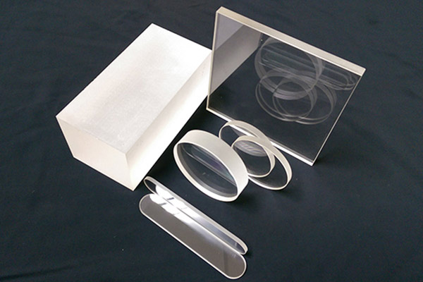
In the ultra-clean, high-precision world of semiconductor manufacturing, wafer fabrication equipment demands components that meet micron-level tolerances, superior material stability, and extreme process consistency. These parts – from electrostatic chucks and vacuum suction plates to spin coating heads and wafer carriers – play a critical role in ensuring cleanroom compatibility, thermal stability, and chemical resistance.
✔ Challenges in Precision Machining of Wafer Fab Equipment Components
The complexity of machining wafer fabrication parts lies in:
- Ultra-tight tolerances: Dimensional tolerance often reaches ±0.001mm, with surface roughness below Ra0.2μm.
- Material fragility or reactivity: Parts made of ceramics, quartz, PEEK, or PTFE are prone to deformation, thermal expansion, or machining damage.
- Complex geometries: Many components feature microholes (≤0.2mm), internal cavities, or extremely thin walls that require simultaneous structural integrity and minimal weight.
- Cleanroom compliance: All parts must be free of particle contamination, burrs, and surface residues.
✔ Materials and How We Maximize Their Performance
To meet such high-end requirements, we precisely select and optimize machining for the following materials:
- Ceramics (Al₂O₃, AlN, ZrO₂): Through ultra-fine grinding and diamond polishing, we achieve high flatness and dielectric consistency in components like electrostatic chucks and alignment blocks.
- Quartz & Glass: Precision laser cutting and fine polishing ensure transparency and resistance to thermal shock in chambers and shower heads.
- PEEK, PTFE, PVDF: For acid/alkali corrosion and low particle emission, we perform high-speed micromilling with anti-static clamping systems.
- SUS316L, Titanium, Aluminum 6061-T6: Vacuum-grade metals are CNC machined and passivated/anodized for enhanced corrosion resistance and cleanroom usability.
✔ Key Machining Capabilities & Equipment
We operate in ISO 9001 and ISO 13485 certified workshops with full ESD control. Our workshop includes:
- 5-axis CNC machining centers – Mikron, DMG Mori, for complex parts with multi-face tolerances
- High-speed turning centers – Mazak and Citizen machines for micro shafts and vacuum fittings
- Ultra-precision grinding – Studer, Waida, enabling roundness within 0.001mm
- Diamond wheel ceramic grinding – Custom rotary & surface grinders for ESC and ceramic holders
- CMM & Roundness testers – ZEISS and Tokyo Seimitsu for inspection within 2μm
- Class 1000 cleaning and packaging rooms – Particle-free post-process handling for cleanroom compliance
✔ 20+ Years of Experience: From Blueprint to Global Success
Over the past two decades, we’ve delivered over 200,000 customized wafer fab components to semiconductor toolmakers and equipment integrators globally. Some examples include:
- ✅ Electrostatic chuck baseplates for a Japanese ALD chamber manufacturer
- ✅ PEEK wafer carriers for a German lithography equipment supplier
- ✅ CVD ceramic parts for an American plasma etch tool integrator
- ✅ SUS precision chucks delivered to fabs in Singapore and Israel
We work directly from customer drawings (PDF/STEP), co-develop custom prototypes with engineers, and ship worldwide within 7–15 working days for standard batches.
✔ Let’s Elevate Your Semiconductor Equipment Together
As the semiconductor industry marches toward 2nm and beyond, part precision, consistency, and cleanliness are no longer optional — they’re fundamental.
Our Chinese precision machining facility combines decades of craftsmanship with modern automation, giving you the reliability, scalability, and technical depth required by today’s top-tier fabs and OEMs.
📩 Contact us today to discuss your wafer fab component needs.