Ultra-Precise Machining for Wafer Handling & Transfer System Components
Empowering Semiconductor Fab Automation with Micron-Level CNC Manufacturing from China
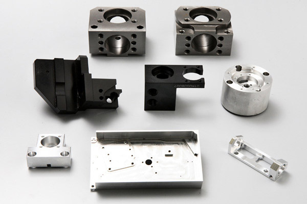
In semiconductor fabs, wafer handling and robotic transfer systems ensure safe, particle-free movement of ultra-thin wafers through dozens of process steps. Whether in FOUP load ports, EFEM arms, or atmospheric robots, the core mechanical components must be extremely lightweight, durable, and dimensionally stable — even after millions of repetitive motions.
With 20+ years of experience, our factory in China specializes in the high-precision machining of robotic arms, end-effectors, linear shafts, sliders, and guide systems tailored for semiconductor wafer handling solutions.
✔ Machining Challenges in Wafer Transfer Mechanisms
Wafer handling components must meet some of the semiconductor industry’s most critical mechanical and cleanliness requirements:
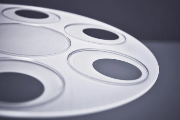
- Micron-level positional accuracy: Deviations >±0.001mm may lead to wafer slippage, misalignment, or breakage.
- Weight vs. rigidity balance: Robotic arms must be extremely lightweight for speed, yet strong enough to resist torsion.
- Burr-free, smooth surfaces: To prevent particle shedding in cleanroom environments, surfaces must reach Ra ≤ 0.1μm.
- Chemical & thermal compatibility: Materials must withstand fab chemicals, ESD environments, and moderate thermal cycles.
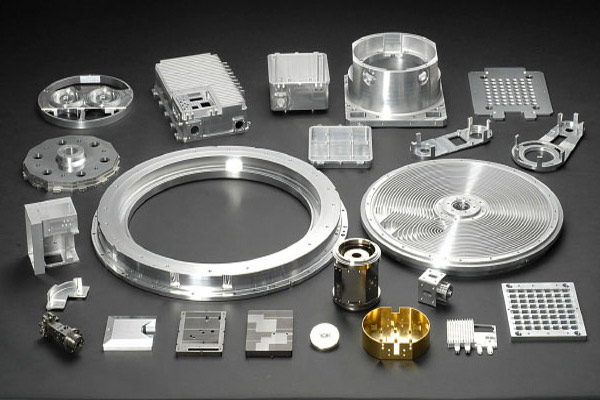
✔ Materials We Use – Engineered for Cleanroom Automation
We select and optimize the following materials based on functional requirements:
| Material | Component | Why We Use It |
|---|---|---|
| Aluminum Alloys (6061-T6 / 7075) | Arm bases, sliders | Lightweight, good machinability, anodizable for anti-corrosion & anti-static |
| Titanium & Alloys | Joint links, pivots | High strength-to-weight ratio, corrosion resistant, ideal for high-load arms |
| PEEK, PTFE, PFA | End-effectors, finger pads | Chemically inert, cleanroom-grade polymers, ESD-safe options available |
| High-Hardness Stainless Steel (SUS440C, SUS630) | Precision shafts, bearing seats | Excellent dimensional stability and wear resistance |
| Ceramics (Alumina / Zirconia) | Isolation mounts, anti-wear joints | Non-conductive, wear-resistant, ultra-smooth |
✔ Our CNC and Inspection Capabilities for Robotic Parts
Our facility is optimized for manufacturing robotic and transfer system parts with ultra-tight tolerances:
- 5-Axis CNC Machining – For complex articulated parts, with tolerance down to ±0.002mm
- Swiss-Type Turning Centers – For small diameter precision shafts and pins (OD tolerance within 0.001mm)
- Mirror Polishing & Deburring – Ensures no particle generation or edge chipping
- Anodizing & Anti-static Coating – For aluminum and polymer parts, optional black hard coat
- Ultrasonic Cleaning & Vacuum Packaging – Class 1000 cleanroom compatibility
Inspection Tools:
- Zeiss CMM for full 3D dimensional verification
- Roundness tester (Tokyo Seimitsu) for shafts and rotary joints
- Surface profiler for Ra/Rz detection
- Material traceability via SGS/COA/RoHS documents
✔ Real-World Projects Delivered to Global Semiconductor Integrators
- ✅ Custom aluminum robotic arm base for a German EFEM unit supplier
- ✅ Titanium pivot joints for a Korean wafer transfer robot manufacturer
- ✅ PEEK end-effectors for a Singaporean FOUP loadport system integrator
- ✅ Linear rail housings delivered to cleanroom automation providers in the USA and Israel
Our team co-develops parts based on your STEP/IGES drawings, offers design-for-manufacturing feedback, and supports fast prototyping (as fast as 7 days) and production scaling.
✔ Why Semiconductor Equipment Companies Trust Us
- 🏭 20+ Years of experience in ultra-precision machining
- 🤖 Full support for motion-critical robotic components under ±0.001mm tolerance
- 🌐 Exported to 30+ countries and trusted by global fabs and OEMs
- 🧼 Cleanroom-ready with Class 1000 cleaning & packaging
- 🛠️ Material mastery across metals, polymers, ceramics — for complex mechanisms
📦 Let’s Engineer Your Wafer Handling Components with Precision
In an industry where 1μm can make or break an entire wafer, choosing the right machining partner is mission-critical. We help you achieve flawless wafer transfer with robotic parts engineered for speed, cleanliness, and stability.
📨 Send us your drawings today and get a quote within 24 hours.